 |
| Classic Amp PCB - Click to Enlarge |
Friday, March 16, 2012
Classic Amp -- Updated PCB, and Why Not?
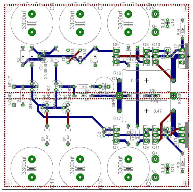
Ok, so I updated the PCB yet again. Check it out:
What did I do? Well, I flipped the transistors Q7, Q9, Q11 and Q13 on the bottom half the board, so that they're a mirror image of Q6, Q8, Q10 and Q12 on the top half. It is now beautifully symmetrical, and the positive and negative pulling devices will have as similar a layout as is physically possible. There's just one problem: Q12 & Q13 are facing opposite directions. Too bad the transistor manufacturers didn't consider this when they made complementary devices - duh! I have it figured out, though: I'm going to sandwich both devices between two heat sinks. Pure symmetry, Captain! You'll just have to wait for the snapshot of the prototype to see what I have planned.
Classic Amp -- Guess What?
That's right folks, it's another iteration of the PCB layout. I wanted to get the drivers closer to the finals, so I rotated the big emitter degeneration output resistors so I could put the finals closer in. That necessitated refactoring both power supply planes. While I was in the market, I put most of the traces on the ground side so they would interrupt the power supply planes as little as possible. Finally, I added a 0.1uf bypass on the power supplies.
There is a lot to be said for multi-layer boards. Life would be simpler if I could put the power and ground planes on an inner layer.
 |
| Refactored PCB - Click to Enlarge |
There is a lot to be said for multi-layer boards. Life would be simpler if I could put the power and ground planes on an inner layer.
Tuesday, March 13, 2012
Classic Amp -- Plagiarism
Some of you, looking at my schematic, might have noticed similarities to this, this, or especially this. The last one has some marked similarities, right down to my R11. I rarely see emitter degeneration in the VA. In my final design, I might make it vanishingly small, or jumper it out altogether, but I wanted to experiment with it, and see what kind of effect it has on distortion, gain and bandwidth. I actually didn't see that schematic until a couple of days ago, when it turned up in a Google search for Sziklai parasitic oscillation.
Although I have the ESP site bookmarked, along with Douglas Self's and Marshall Leach's sites, I promise you that I was working independently when I did the schematic capture.
Of course, there are only a few ways to configure a "classic" amplifier and still have it be, well -- classic. So you should expect some similarities. As I said in my original post, I wanted to include a number of enhanced features, without over designing. There is only one way to make a differential amplifier that has a current source and a current mirror. There are only two typical output configurations: Darlington and Sziklai. The rest is all calculating values, parts selection, testing performance and optimization.
The area that lends itself to originality is the PCB layout. Although there's really nothing original about ground and power planes, I have never seen a power amp use them. I'm using Eagle Light for this project, so I can only do two layer boards. Otherwise, I would have done a four layer board, with power and ground on the two interior layers (V+ and V- planes could almost meet in the middle), and signal traces on the two outer layers.
But I think the other thing that makes this board unique is the ability to make the temperature compensation track by fastening together Q8 & Q10 and Q9 & Q11.
I think that the power and ground planes might make this amplifier more stable, requiring less tweaking (fewer caps, or lower values) to control oscillation. Stay tuned. I believe this will be an unique amplifier.
 |
| Classic Amp - My Schematic - Click to Enlarge |
Although I have the ESP site bookmarked, along with Douglas Self's and Marshall Leach's sites, I promise you that I was working independently when I did the schematic capture.
Of course, there are only a few ways to configure a "classic" amplifier and still have it be, well -- classic. So you should expect some similarities. As I said in my original post, I wanted to include a number of enhanced features, without over designing. There is only one way to make a differential amplifier that has a current source and a current mirror. There are only two typical output configurations: Darlington and Sziklai. The rest is all calculating values, parts selection, testing performance and optimization.
The area that lends itself to originality is the PCB layout. Although there's really nothing original about ground and power planes, I have never seen a power amp use them. I'm using Eagle Light for this project, so I can only do two layer boards. Otherwise, I would have done a four layer board, with power and ground on the two interior layers (V+ and V- planes could almost meet in the middle), and signal traces on the two outer layers.
But I think the other thing that makes this board unique is the ability to make the temperature compensation track by fastening together Q8 & Q10 and Q9 & Q11.
 |
| Classic Amp - My PCB - Click to Enlarge |
Sunday, March 11, 2012
Classic Amp Updated Board IV
Just when you (meaning I) thought it couldn't get any smaller or cleaner, I spy another opportunity for optimization.
- I moved Q6 & Q7 in line with the drivers (Q10 & Q11), which shortened the traces considerably, and made it possible to shrink the whole design once again.
- The size of the board being determined by the big filter caps, I decided to drop two of them, and increase the value of the remaining ones. Four 2200uf are now three 3300uf (which actually increased the total from 8800uf to 9900uf per side). The Panasonic data sheet says 3300uf fit in this footprint.
- I also added a power ground pad next to each power input pad. Both ground lines will go back to the transformer center tap, but this way, the ripple current will go to the associated filter caps, and not have to flow across the ground plane.
- While I was moving grounds around, I decided to move the speaker ground where it would be centered on the board, so the current flow would be more symmetrical through the ground plane.
|
| Great Grandson of Updated PCB - Click to Enlarge |
Anyone want to wager on how many more iterations there are?
One final thought: There might be a bit of ripple at Q12 & Q13, or R14 & R15. I don't think this will be a problem, since the output voltage will be governed by Q10 & Q11. Any perturbations in the supply to the output devices would be compensated by the local feedback inherent in the Sziklai configuration. Still, I would have preferred to have the raw rectifier output hit a capacitor before it hits my output transistors. Even with the big fat power supply rail, there is still some resistance between P+ and C6, et. al. For this reason, there might be some justification for a bit of off-board filtration. I'm just sayin'.
|
| Updated Schematic - Click to Enlarge |
Classic Amp Updated Board III
I have made some more optimizations to the board.
- Shortened leads by dodging corners
- Compacted the power amp section to shorten leads
- Changed the feedback capacitor (C1) from axial to radial, dramatically saving board real-estate.
- Pulled in the input section to fill in the vacant real-estate.
 |
| Grandson of Updated PCB - Click to Enlarge |
I could make it smaller yet, but then the silkscreen parts nomenclature would become more of a mess than it is already. This is probably small enough. The filter caps are as compact as they're going to get anyway. So unless we want to abandon the power plane and bypass idea, I think we're at our physical limit, for the most part.
Saturday, March 10, 2012
Classic Amp Updated Board II
I made some more changes to the board layout:
- Moved the power planes to the top side of the board, so I could make the ground plane fill the entire bottom side, and so I could significantly widen the power planes. It also allowed the power planes to flow to the output transistor power connections, instead of having to route to it (higher current capacity).
- Widened speaker output trace (higher current capacity).
- Increased clearance to output transistor pads.
- Eliminated vias -- now using component mounting holes to switch sides if needed.
 |
| Son of Updated PCB - Click to Enlarge |
Classic Amp Updated Board
I fixed up some awkward routing, and a couple of dimension errors on some parts. It's always a good idea to double check the spec sheets before releasing a PCB to manufacturing. Once it's etched and drilled, it's too late.
 |
| Updated PCB - Click to Enlarge |
Friday, March 9, 2012
Classic Amp Schematic and Board
 |
| Schematic - Click to Enlarge |
 |
| Board - Click to Enlarge |
Monday, March 5, 2012
Classic Amp Schematic (Preliminary)
 |
| Schematic (click to enlarge) |
Differential Amplifier
The differential amplifier compares the input voltage with the output voltage via the feedback network, R8, R9 and C1. Any difference between the two voltages creates an error correction signal for the voltage amplifier. Q2 and Q3 are the differential amplifier. Q1 is the current source for the differential amplifier. Q4 and Q5 are the current mirror, so that the voltage amplifier, Q7 gets the benefit of both Q2 and Q3 from the differential amplifier.
D1 and D2 are the voltage reference for the current sources. R2 sets the differential amplifier at about 20 mA, or 10 mA per device. R5 and R6 set the voltage at Q7 base at about 1.2 volts. This will approximately balance the differential amplifier. R3 and R4 are placeholders that will be determined experimentally to provide the correct amount of emitter degeneration to reduce the open loop gain of the amplifier to the desired amount, and linearize the differential amplifier.
Voltage Amplifier
The voltage amplifier is responsible for providing the bulk of the voltage amplification (when compared to the few millivolt swing from the diff amp, and the nominally unity voltage gain of the output stage). Voltage amplifier Q7 works into constant current source Q6. R10 sets Q6 to provide approximately 10 mA. R11 sets Q7 base to approximately 1.2 volts at 10 mA, consistent with the current mirror at Q4. R11 provides emitter degeneration to linearize the voltage amplifier. R5, R6 and R11 are placeholders that will be determined experimentally for optimum open loop gain and linearity. They will all be chosen to balance the differential amplifier when idling. C2 provides the dominant pole for setting the power bandwidth and phase margins of the amplifier. The optimal value will be determined experimentally.
Power Output Stage
Q10 and Q11 are the pseudo emitter-followers for the output stage. They're connected as emitter followers, except that they get a power assist from Q12 and Q13, which are the actual power output devices. This is the Sziklai configuration. Being inside the local feedback loop established by Q10 and Q11, the current through Q12 and Q13 is entirely controlled by Q10 and Q11. Therefore, it is only necessary to temperature stabilize Q10 and Q11 -- and since Q10 and Q11 dissipate much less power than Q12 and Q13, temperature stabilization and thermal runaway are much less of a problem, and very easily controlled. R14 and R15 speed up the output bandwidth, and set the idling current of Q10 and Q11 at about 10 mA, to match Q8 and Q9 when idling. Finally, C3 and C4 may be required to control any tendency of the output stage to oscillate. The actual value, if needed at all, will be determined experimentally.
Bias and Temperature Compensation
R12 and R13 bias the output stage; Q8 and Q9 are diode-connected to provide temperature compensation for Vbe of Q10 and Q11. Diodes are normally used in place of Q8 and Q9, but Q8 and Q10, Q9 and Q11 can be placed on the board in close proximity so that they can be fastened together for excellent temperature tracking. With the temperature compensation from Q8 and Q9 and the constant current from Q6, the quiescent idle current through Q12 and Q13 is completely determined by R12 and R13. The values are chosen to idle the finals at about 20 mA, which is a little on the low side for class AB (see equation 21). I might increase R12 and R13 to about 2.2 Ohms, for an idle current of about 50 mA later on.
Feedback
Overall feedback is provided by R8, R9 and C1, and is applied only after the open loop linearity and bandwidth, slew rate, etc. have been optimized. The rule for good amplifier design is, minimize open loop distortions, and then apply feedback. Then the feedback will set the gain at about 26 dB, and further linearize the amplifier.
Leaving Options
There are a number of place holders in this design, so that the circuit board will have places for all the options. They can be left empty or jumpered out if not needed. After the PCB is manufactured, it is easier to eliminate extra parts than it is to add extra ones.
A Classic Audio Amplifier
I have always wanted to design a "classic" audio amplifier. One that is "no compromise", meaning that it has everything it needs, and nothing it doesn't. Due to cost or time constraints, I have designed amplifiers in the past that have been sub-optimal. I remember one in particular: It was a studio amplifier for a radio station. It was about 20 watts, and used the usual differential input, a voltage amplifier, and a current amplifier output stage. But, it was the simplest thing that could possibly work -- there were compromises.
- The diff amp used a simple resistor current source, and it had a simple resistor output stage.
- The voltage amplifier was connected to the diff amp's non-inverting output; the inverting output was ignored (a common practice).
- The voltage amplifier used a resistor as the current source; it did not have an active current source, or a "bootstrap" to regulate the current.
- The voltage amplifier also did not have a Cdom capacitor to establish a dominant HF pole (for feedback stability).
- The output stage used a couple of internally connected Darlington transistors instead of discrete parts for the emitter follower output.
- Add a current source to the diff amp.
- Add a current mirror to the diff amp (to use the output from both transistors in the long-tailed pair).
- Add a current source to the voltage amp. I prefer a current source over bootstrapping, although I have seen some very good amplifiers use bootstrapping. I just think a current source may be more reliable and less dodgy to analyze.
- Add Cdom to the voltage amp, to establish a dominant HF pole to design around, and set predictable phase margins for feedback.
- Use Sziklai configuration for the current output stage, using discrete parts.
The Sziklai configuration does have the potential to oscillate, whereas a Darlington emitter follower doesn't, but that is fairly easy to control, and the thermal stability advantage seems to more than make up for it.
I will be blogging the development of a 40 ~ 60 watt design in the upcoming weeks and months. I'll post a preliminary schematic soon.
Subscribe to:
Posts
(
Atom
)